PRODUCTS
About Our Technology
Gypsum
Ceramic cores
Porous ceramic component
Decoration Materials
Thick Film Circuit Substrate
- Thick Film Circuit Substrate with Precious Metal design guidance
- About Our Technology
- New Copper Conductors + Plating Substrate design guidance
- Thick Film Circuit Substrate with Copper Conductors design guidance
- Thick Film Heater design guidance
- Catalog Download
- About Our Sales Offices
About Our Thick Film Manufacturing Technology
Gold-plated Printed Substrates
Printed circuit substrates with silver conductor traces can be plated with gold.
This results in excellent soldering and wire bonding characteristics.
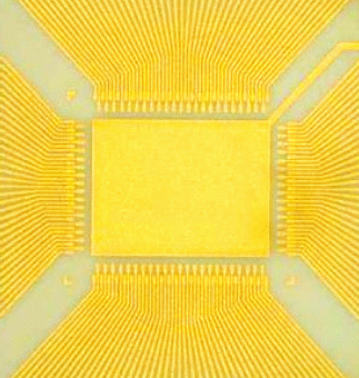
Long-length Substrates
Thick film circuits can be formed on ceramic substrates up to 310 mm in length.
Substrate size: 310 mm × 95 mm maximum
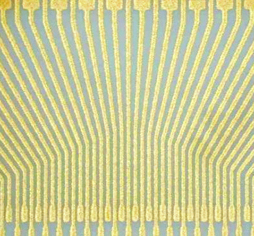
Fine Line Printing
Minimum lines and spacing: 50 μm / 50 μm
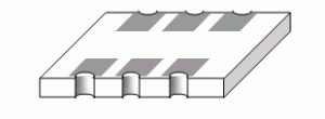
Castellation
Circuit substrates can be castellated to support surface mount devices.
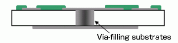
Via-filling Substrates
Via-filling substrates can handle higher current levels than ordinary through-hole substrates.
They are also effective in raising heat dissipation with thermal vias.