

News Release
9/2/2026
NORITAKE CO., LIMITED
Development of Diamond-Abrasive-Embedded Polishing Pad for Semiconductor Applications
– Contributing to Larger SiC Wafers and Reduced Industrial Waste –
NORITAKE CO., LIMITED (Headquarters: Nagoya, Aichi; Representative Director and President: Akira Higashiyama) has developed LumiDia, a diamond-abrasive-embedded polishing pad used in polishing processes for the manufacture of silicon carbide (SiC) wafers and other semiconductor materials. Featuring a proprietary structure that incorporates diamond abrasives within the pad, LumiDia achieves excellent polishing performance and enables edge polishing of SiC wafers, which has been difficult to achieve using conventional diamond slurry-based polishing methods. Because polishing can be performed using only water, the product also contributes to the reduction of industrial waste.
Market Environment
In recent years, the advancement of autonomous driving technologies and the growing adoption of electric vehicles (EVs) have driven increasing demand for power semiconductors capable of handling high voltages and large currents. In the manufacturing process of SiC wafers used for such semiconductors, polishing plays a critical role in flattening wafer surfaces and reducing surface roughness. To efficiently process hard and brittle materials, polishing using diamond slurry*1 is commonly employed. However, slurry must be continuously supplied during polishing, and the used slurry becomes industrial waste. In addition, concerns regarding the stable procurement of diamond abrasives have increased, making the reduction of abrasive consumption an important challenge.
Challenges in SiC Wafer Manufacturing Amid the Shift to Larger Diameters
As SiC wafers continue to increase in size from 6 inches to 8 inches, improving yield has become increasingly important due to the greater number of semiconductor chips that can be produced from a single wafer. As a result, improving the precision of wafer edges has emerged as a key challenge. If the surface roughness of the wafer edge is too high, the risks of chipping, cracking, and particle contamination increase, potentially affecting device performance, reliability, and manufacturing yield. However, because wafer edges have a curved geometry, diamond slurry is difficult to retain in the polishing area. This significantly reduces polishing efficiency when processing hard and brittle materials such as SiC, creating a need for advanced edge-polishing technologies.
Product Features
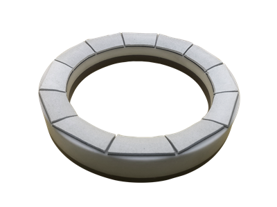
LumiDia is a diamond-abrasive-embedded polishing pad that requires only water during the polishing process. Noritake has been developing polishing pads containing abrasives by leveraging its proprietary technology for combining organic and inorganic materials. This technology has also been applied to LumiDia, which is designed with a structure that enables the diamond abrasives embedded within the pad to function efficiently. As a result, the pad achieves high polishing performance while using only a small amount of diamond abrasives.
Enabling Edge Polishing of SiC Wafers and Supporting Larger-Diameter Wafer Production
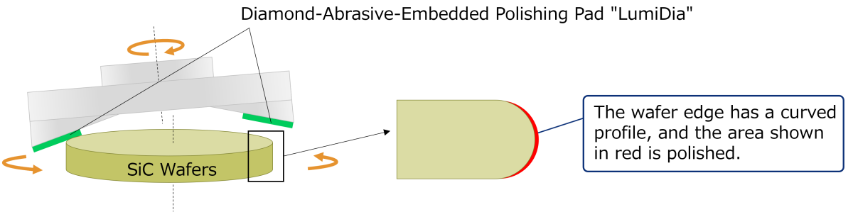
LumiDia enables edge polishing of SiC wafers, a process that has been difficult to achieve using conventional diamond slurry. By reducing wafer chipping, cracking, and particle contamination, LumiDia helps improve manufacturing yield and contributes to the stable supply of 8-inch SiC wafers, whose adoption continues to expand. Furthermore, because polishing can be carried out using only water, the product helps reduce industrial waste.
<Image of the Edge Polishing Process*2>
Applicable to Various Polishing Processes
In addition to edge polishing of SiC wafers, LumiDia can also be used for surface polishing of ceramic substrates, where it enables reduced diamond abrasive consumption and extended polishing pad life. Leveraging these advantages, Noritake will continue exploring broader applications in the semiconductor industry.
*1 Diamond abrasives dispersed in an aqueous solution or other liquid medium. Diamond slurry is widely used for polishing hard materials.
*2 Illustration based on the edge-polishing method developed by BBSKINMEI CO.,Ltd. a manufacturer of semiconductor-related equipment.