News Release
8/20/2025
NORITAKE CO., LIMITED
Successful Development of Polishing Pads for GaN Wafers
- Contributing to Higher Productivity in Semiconductors for High-Speed 5G/6G Communications -
NORITAKE CO., LIMITED (Headquarters: Nagoya, Aichi; Representative Director and President: Akira Higashiyama) has developed a polishing pad for gallium nitride (GaN) wafers used for applications such as high-speed communications. This newly developed product shortens GaN wafer processing time and significantly extends the product lifespan, contributing to the reduction of industrial waste.
Market Environment
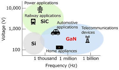
In high-speed communication standards such as 5G, high-frequency radio waves are used. Therefore, communication devices*1 used in base stations and data centers require fast and stable operation at high frequencies. Research is underway to expand the use of GaN semiconductors, which can operate at higher frequencies and withstand high voltage and large currents.
Challenges in Manufacturing GaN Wafers
In the manufacturing process of communication devices, it is necessary to polish and planarize the surface of semiconductor wafers using a polishing pad to form fine circuits on the wafer. However, GaN is a very hard and brittle material, making the polishing process difficult and time-consuming in order to achieve a flat surface.
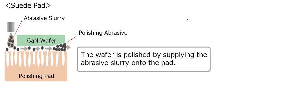
To polish GaN wafers in a short time, processing in a strongly acidic environment (pH*2 1–2) is required. However, commonly used polishing pads in the semiconductor industry (suede pads) cannot withstand such acidic conditions and deteriorate during use.
Additionally, in conventional polishing methods, the polishing slurry*3 is supplied onto the surface of the pad during polishing. Since this slurry becomes industrial waste after use, reducing its consumption is essential.
Product Features
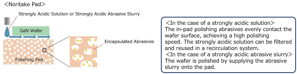
Noritake has developed a polishing pad that withstands strongly acidic environments using its proprietary technology that combines organic and inorganic
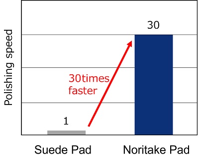
① Thirtyfold Increase in Polishing Speed*4
By using a highly acid-resistant resin, the pad can be used under strongly acidic environments, resulting in faster polishing and shorter processing times.
② Pad Service Life Extended to More Than 15 Times*4
Pad wear is reduced by encapsulating the abrasive (inorganic material) within an acid-resistant resin (organic material). Furthermore, conditioning the pad surface maintains polishing performance even as the pad wears, thereby significantly extending the pad’s service life.
③ Reduction of Industrial Waste
・Reduction in polishing processing time reduces the amount of polishing slurry used.
・Encapsulated abrasives allow polishing without using slurry.
・Extended lifespan reduces the number of discarded pads.
Performance Comparison (Results of In-House Testing)
Polishing test was performed under the following conditions:
Suede Pad: pH 10 (weak alkaline region)
Noritake Pad: pH 1 (strong acidic region)
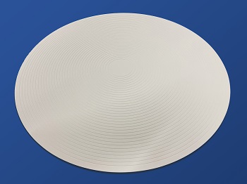
Pad Structure
*1 Devices mainly used within computers for transmitting and receiving data.
*2 A cale that indicates acidity or alkalinity. Below 7 is acidic, and the smaller the number, the stronger the acidity.
*3 A dispersion of abrasive particles in an aqueous solution.
*4 Polishing was performed under the following conditions:
Suede Pad: pH 10 (weakly alkaline region)
Noritake Pad: pH 1 (strongly acidic region)