News Release
9/11/2025
NORITAKE CO., LIMITED
Launch of Copper Nano Paste and Slurry for Semiconductor Circuit Formation
- Copper nanoparticles scaled up by Noritake will be marketed in collaboration with Mitsubishi Corporation Group -
NORITAKE CO., LIMITED (Headquarters: Nagoya, Aichi; Representative Director and President: Akira Higashiyama) will begin sales of paste and slurry containing copper nanoparticles that can be sintered at temperatures of 200°C or lower in a nitrogen atmosphere*1. This product was commercialized by scaling up the production of copper nanoparticles developed by Hokkaido University using Noritake’s fine particle manufacturing technology. In collaboration with the Mitsubishi Corporation Group, Noritake will promote sales of these products for semiconductor module circuit formation applications.
Market Environment
In the production of printed circuit boards, electronic circuits are typically formed using photolithography*2, where a copper film is formed over the entire substrate and unnecessary portions are removed with chemicals to form circuit patterns. However, much of the removed copper is often discarded. Additionally, the chemicals used are highly corrosive and raise environmental concerns, so there is a demand to reduce their usage.
In contrast, electronic circuit formation by printing copper paste, a method that has been increasingly studied in recent years, enables reduction of material usage because the paste is only applied to necessary areas and does not require chemicals. However, this approach requires sintering*3 at 300℃ or higher during wiring formation, which may cause warping or degradation of the printed circuit board due to heat. These issues are particularly critical for advanced semiconductors, where lamination or thinning is required, making it essential to minimize substrate warping and degradation. Against this backdrop, efforts have been made to develop paste using copper nanoparticles that can be sintered at lower temperatures.
Challenges with Copper Nanoparticles
Copper nanoparticles have organic materials and copper oxide layers on their surfaces, which hinder sintering. Therefore, it is necessary to sinter at over 300°C using hydrogen or formic acid gas to remove these surface layers. However, because these gases are flammable, they pose safety challenges in manufacturing environments.
Characteristics of the Scaled-Up Product
① Can be sintered at 150–200°C under nitrogen atmosphere
By forming a specialized, easily reducible coating on the particle surface, the product enables low-temperature sintering under an inert nitrogen gas atmosphere. This helps minimize warpage and degradation while reducing safety management burdens.
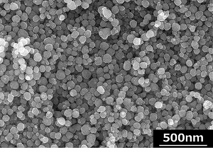
② Uniform particle size of 100 nm or less
Particles uniformly sized at 100 nm or less are dispersed within the paste using advanced dispersion technology. This enables the particles to pack densely without gaps, resulting in dense wiring after sintering.
These features enable the paste to support multilayer and thinner printed circuit boards, contributing to improving semiconductor module performance. Adopting paste printing for electronic circuit formation reduces copper usage compared to photolithography and reduces environmental impact by eliminating the use of chemicals.
Applications
・Wiring for electronic circuits in semiconductor modules
・Bonding material for semiconductor chips
Future Market Expansion
For future sales development, we will collaborate with the global sales networks of Mitsubishi Corporation and its group company MC Yamasan Polymers Co., Ltd., a specialized trading company handling semiconductor materials and other chemicals, to expand our customer base.
*1 An environment consisting mainly of nitrogen gas.
*2 A technology for forming circuits by applying photosensitive materials and exposing them in patterned light.
*3 A process that leads to dense bonding through sintering. In metals, this lowers resistivity and enhances electrical conductivity.