News Release
12/11/2025
NORITAKE CO., LIMITED
Development of Silver Paste for TGV Supporting the AI Era
- Toward Practical Use of Glass Substrates for Advanced Semiconductor 3D Packaging -
NORITAKE CO., LIMITED (Headquarters: Nagoya, Aichi; Representative Director and President: Akira Higashiyama) has developed a silver paste for Through Glass Via (TGV)*¹ used to form interconnect through substrates in 3D-packaged semiconductor devices. This technology enables massive computational processing and contributes to the spread and expansion of AI technology. The newly developed product will be exhibited at SEMICON JAPAN 2025, starting on December 17.
Market Environment
AI servers consume enormous amounts of power due to massive computational processing. As AI continues to spread and expand, achieving both high-speed processing and low power consumption has become essential. To address this challenge, demand for advanced semiconductor packages that are thinner and stacked in 3D configurations is increasing.
Technology Development for Practical 3D Packaging
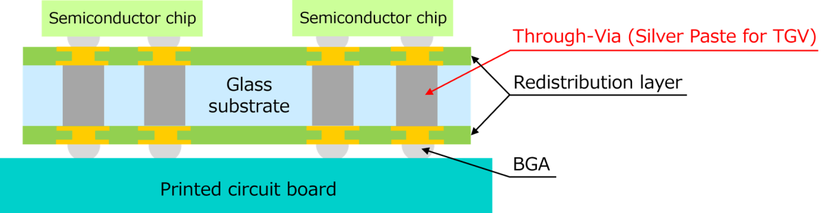
In advanced semiconductor packages with 3D Packaging, a core substrate*² is placed between the semiconductor chip and the printed circuit board, and through-vias (holes for interconnect ) are drilled and formed to connect them.
During semiconductor operation, temperatures can reach up to approximately 300°C, which may cause warping or degradation in conventional resin substrates. To overcome this issue, development is underway to use heat-resistant glass as the core substrate.
Challenges in Utilizing Glass Substrates
For practical implementation of TGV interconnect in glass substrates, copper plating technology has been considered promising. However, it faces challenges such as long processing times and a tendency for cracks to form in the vias.
Highlights of the Newly Developed Product
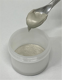
The newly developed product is a silver paste for TGV that solves the issues of copper plating technology. By employing proprietary composition design and particle dispersion technology, the amount of silver particles has been maximized, achieving resistance values equivalent to conventional copper plating while significantly improving interconnect process efficiency.
① Processing Time Reduced to One-Fifth
Interconnect is formed by filling the through-via with silver paste and sintering it, dramatically shortening processing time. Pre-treatment steps required before plating are also eliminated.
② Contributes to Defect Reduction
The composition and particle dispersion technology, which withstand temperature changes during semiconductor operation, help suppress crack formation*³.
By using this silver paste for interconnect, the adoption of heat-resistant glass substrates will be promoted, enabling faster processing and lower power consumption in advanced semiconductor packages, thus contributing to further AI proliferation.
Application Areas of the Developed Product
*1 Forming interconnects by drilling vertical holes in a glass substrate to electrically connect different layers.
*2 A substrate that connects the semiconductor chip and printed circuit board, transmitting electrical signals and supplying power while enhancing package strength.
*3 In a thermal shock test cycling between -65°C (30 minutes) and 125°C (30 minutes) for 100 cycles, no cracks were observed.