- HOME
- Product Information
- Engineering
- Filtration Systems
- Ceramic filter
- Ceramic filter For Electronics and Semiconductors
PRODUCTS
Ceramic filter For Electronics and Semiconductors
Engineering
-
Heating Furnaces / Kilns
- Heating Furnaces / Kilns List
-
Drying Furnace
- Drying Furnace List
- Batch Kiln
- Far Infrared Conveyer Furnace
- Other Drying Furnaces
- Roll to Roll Far-infrared Heating Furnace
- Far Infrared Heater
-
Firing Kiln
- Firing Kiln List
- Roller Hearth Kiln
- Pusher Kiln
- Rotary Kiln
- Other
- Batch Kiln
- Refractory
-
Search by industry or usage
- Search by industry or usage List
- Semiconductors
- Energy
- Electronics
- Automobiles
- Displays and lighting
- Other
- Furnace Construction Maintenance
-
Mixing Technology
- Mixing Technology List
-
SM Engineering Equipment
- SM Engineering Equipment List
-
Heating and Cooling Systems
- Heating and Cooling Systems List
- Saccharification system for bio-ethanol production
- Adhesive Temperature Adjusting System
- Coating Liquid Precision Temperature (viscosity) Adjusting System
- Scrambled Eggs Continuation Manufacturing System
- Condiment Miso Heat Sterilization System
- Starch Gelatinization System for Paper Manufacturing
- Flour Paste Manufacturing System
- PVA Continuous Dissolution System
- Seasoning Liquid Heating Sterilization Cooling System
- Automated Oxidized Starch Production System
- In-line Starch Saccharification System
- Water Heating System
- Mixing Systems
- Powder and Liquid Dispersion System
- Reaction System
- Laboratory Test Systems
-
Heat Exchangers
- Heat Exchangers List
- Heat Exchangers
- Reaction
-
Static Mixer (SM)
- Static Mixer (SM) List
- Gas absorption(Option)
- Homogenization
- Miixing
- Option Parts
- Cooker / Steam Mixer
- Cutting Machine (Thin Cut Master : TCM)
-
Filtration Systems
- Filtration Systems List
- Search lubricants
-
Coolant Filtration Systems
- Coolant Filtration Systems List
- Centrifuge
- Magnetic Separator
- Cyclone Separator
- Paper Filter
- Backwash Filter
- Search by industry or usage
- Search filtration materials
- Filtration Related Systems
- Ceramic filter
- Technical Support
- Catalog Download
- About Our Sales Offices
Technical Support
It reduces the amount of water intake and drainage used in the semiconductor / liquid crystal manufacturing process.
Stable operation facilitates operation management and maintenance.
[Filtration] [Recovery] [Separation] [Concentration] [Purification]
Option
- Filtrate tank
- Two-stage concentration unit
- Filter cleaning chemical injection unit
- Clean room compatible unit
- Heat exchange unit
Features
By filtering and collecting the wastewater, the amount of wastewater can be drastically reduced.
- 99.9% or more of the filtered liquid can be expected to be recovered from the DC processed wastewater.
- 99.5% or more of the filtered liquid can be expected to be recovered from BG processed wastewater.
- 99% or more of the filtrate can be expected to be recovered from CMP wastewater.
By using the filtrate as the raw water of the pure water device, the load on the pure water device can be reduced.
By circulating water, the amount of water intake and drainage can be drastically reduced.
There are no consumables and running costs can be reduced.
There is no damage to the filter, which makes operation management easier.
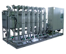
Delivery example
| Application | Silicon wafer DC processing Wastewater recovery |
|---|---|
| Model | 7M3-2S3P |
| Filter | MBX3-1020-0.1 (Membrane pore size: 0.1 μm) |
| Filtration area | 14.7m2 |
| Processing amount | 5.5m3 / h |
| Wet contact material | SUS304 (inner and outer surface pickling |
| Weight | 3200 kg (operating weight) |
| Ancillary equipment |
|
Main application
- BG processed wastewater, DC processed wastewater, CMP wastewater
- Polishing drainage for glass lenses
- Purification and concentration recovery of electronic pastes and slurries
Specification
| Main wastewater permeation flux (FLUX) | Membrane pore size | Permeation flux (l / m2h) |
|---|---|---|
| DC processing drainage for glass/lenses | 0.2 μm | 400-600 |
| DC processing wastewater for silicon/gully arsenic wafers | 100nm | 300-500 |
| BG processing wastewater for silicon/gully arsenic wafers | 100nm | 200-400 |
| CMP (oxide film) wastewater | 50nm | 50-100 |
| CMP (metal) drainage | 50nm | 50-100 |
We will design according to the customer's specifications, so please contact us.